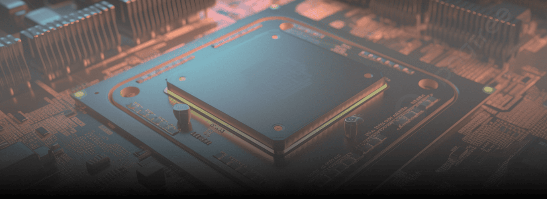
What is Printed Circuit Board (PCB) Design?
PCB Design refers to the process of designing the layout and structure of a Printed Circuit Board, which is used to physically support and electrically connect electronic components. The design involves schematic capture, component placement, routing of electrical connections (traces), and generating files for manufacturing (such as Gerber files).
Uses and Purposes of PCB Design
Uses:
Electronics Manufacturing: Core component in all electronic devices (phones, computers, TVs, etc.)
Automotive Industry: Used in engine control units, sensors, and infotainment systems
Medical Devices: For diagnostic machines, monitoring systems, etc.
Aerospace & Defense: In radar systems, satellites, communication systems
Industrial Machinery: Controllers, automation systems, and sensors
Purposes:
To ensure reliable electrical connectivity among components
To reduce wiring complexity
To enhance durability and performance of electronic devices
- To allow for mass production of electronic devices with consistent quality
Benefits & Advantages of PCB Design
Benefit | Description |
| Compact Size | Reduces space by embedding all components and connections in layers |
| Reliability | Improves device stability and reduces loose connections |
| Ease of Repair | Components are clearly labeled and placed, easing diagnostics and repair |
| Mass Production Friendly | Streamlined design allows for efficient manufacturing |
| Improved Performance | Shorter electrical paths, reduced interference, better signal integrity |
| Cost-Effective | Reduced material cost and labor over time |
How PCB Design Helps Engineering Candidates
Skill Relevance: PCB design is essential in electrical, electronics, mechatronics, and instrumentation engineering.
- Industry Readiness: Teaches hands-on skills in CAD tools like Altium Designer, Eagle, KiCad, OrCAD.
- Project Development: Helps students create their own circuits for academic and real-world projects (e.g., robotics, IoT, embedded systems).
- Innovation and Prototyping: Enables faster prototyping of hardware startups or R&D projects.
Cross-functional Knowledge: Builds understanding of signal integrity, power management, EMC/EMI, and thermal considerations.
Job Titles After Learning PCB Design
Entry-Level | Mid to Senior Level | Specialized/Advanced |
| PCB Design Engineer | Senior PCB Layout Engineer | Signal Integrity Engineer |
| Electronics Design Engineer | Hardware Development Engineer | High-Speed PCB Design Specialist |
| PCB Layout Designer | Embedded Hardware Engineer | RF PCB Design Engineer |
| Junior Hardware Engineer | Product Development Engineer | PCB Manufacturing Process Engineer |
| PCB CAD Technician | Circuit Design Engineer | PCB Reliability/Test Engineer |